(China (Mainland))

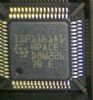
Product Summary
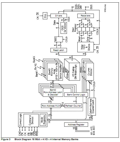
The HYB25D256160CC-5 is a 256 Mbit Double-Data-Rate SDRAM. It is a high-speed CMOS, dynamic random-access memory containing 268,435,456 bits. The HYB25D256160CC-5 is internally configured as a quad-bank DRAM. The 256 Mbit Double-Data-Rate SDRAM HYB25D256160CC-5 uses a double-data-rate architecture to achieve high-speed operation. The double data rate architecture is essentially a 2n prefetch architecture with an interface designed to transfer two data words per clock cycle at the I/O pins. A single read or write access for the 256 Mbit Double-Data-Rate SDRAM effectively consists of a single 2n-bit wide, one clock cycle data transfer at the internal DRAM core and two corresponding n-bit wide, one-half-clock-cycle data transfers at the I/O pins.
Parametrics
HYB25D256160CC-5 absolute maximum ratings: (1)Voltage on I/O pins relative to VSS, VIN, VOUT: –0.5 to VDDQ+0.5 V ; (2)Voltage on inputs relative to VSS, VIN: –1 to +3.6 V; (3)Voltage on VDD supply relative to VSS, VDD: –1 to +3.6 V; (4)Voltage on VDDQ supply relative to VSS, VDDQ: –1 to +3.6 V; (5)Operating temperature (ambient), TA: 0–+70℃; (6)Storage temperature (plastic), TSTG: -55 to +150℃; (7)Power dissipation (per SDRAM component), PD: 1.5W; (8)Short circuit output current, IOUT: 50mA typ.
Features
HYB25D256160CC-5 features: (1)Double data rate architecture: two data transfers per clock cycle; (2)Bidirectional data strobe (DQS) is transmitted and received with data, to be used in capturing data at the receiver; (3)DQS is edge-aligned with data for reads and is center-aligned with data for writes; (4)Differential clock inputs (CK and CK); (5)Four internal banks for concurrent operation; (6)Data mask (DM) for write data; (7)DLL aligns DQ and DQS transitions with CK transitions; (8)Commands entered on each positive CK edge; data and data mask referenced to both edges of DQS; (9)Burst Lengths: 2, 4, or 8; (10)CAS Latency: 1.5 (DDR200 only), 2, 2.5, 3; (11)Auto Precharge option for each burst access; (12)Auto Refresh and Self Refresh Modes; (13)RAS-lockout supported tRAP=tRCD ; (14)7.8 μs Maximum Average Periodic Refresh Interval; (15)2.5 V (SSTL_2 compatible) I/O; (16)VDDQ = 2.5 V ± 0.2 V (DDR200, DDR266, DDR333); VDDQ = 2.6 V ± 0.1 V (DDR400); (17)VDD = 2.5 V ± 0.2 V (DDR200, DDR266, DDR333); VDD = 2.6 V ± 0.1 V (DDR400); (18)P-TFBGA-60-12 package with 3 depopulated rows (8 × 12 mm2); (19)P-TSOPII-66 package; (20)Lead- and halogene-free = green product.
Diagrams
 |
 HYB25L256160AF |
Other |
|
Data Sheet |
Negotiable |
|
||||
|
HYB25L256160AC |
Other |
|
Data Sheet |
Negotiable |
|
||||
|
HYB25DC512800DF-6 |
Other |
|
Data Sheet |
Negotiable |
|
||||
|
HYB25DC512800DF-5A |
Other |
|
Data Sheet |
Negotiable |
|
||||
|
HYB25DC512800DF-5 |
Other |
|
Data Sheet |
Negotiable |
|
||||
|
HYB25DC512800DF-4 |
Other |
|
Data Sheet |
Negotiable |
|
||||